Energy-Band Concepts Of Materials
Energy-band Concepts of Materials
- The electron energy levels for a single free atom in a gaseous medium are discrete, since the atoms are sufficiently far apart. So the energy levels of individual atoms are not perturbed.
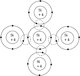
- The proximity of neighbouring atoms in solid media such as crystals does not appreciably affect the energy levels of inner shell electrons. But, groups of energy levels of outer shell electrons are changed due to the influence of electrons in the neighbouring atoms. They allow sharing of electrons among them to form covalent bonds between neighbouring atoms in the process of getting on to stable ‘8-electron configuration’ in Silicon and Germanium semiconductors.
Sharing of outer shell electrons to form covalent bonds is shown in Fig. 2.5.
- Valence band The coupling between the outer shell electrons of the atoms results in a group or a band of closely spaced energy levels or states instead of the widely spaced energy levels of the isolated atoms. Because of the coupling between atoms in the crystals (As the inter-atomic distance is quite small in solid materials.) completely filled and partially filled energy levels are merged into an ‘energy band’ known as Valence Band.
- Top most energy level of Valence Band is EV.
- Merging of empty energy levels in atoms form Conduction Band (top energy band).
- Lower most energy level of Conduction Band is EC.
- Region between Conduction Band and Valence Band is known as forbidden band gap EG, or band gap equal to (EC – EV). It decreases with temperature.
- The magnitude of the band-gap energy EG predicts the type of the materials, such as conductors, semiconductors and insulators, which is discussed later.
- Energy-band diagrams (EBD) show the energy of electrons (in electron volts) associated with the energy levels on the y axis and the momentum (P) on the x axis. Energy of electrons is measured in eV (electron volts).
- The unit of electron volt (eV) is the energy acquired by an electron while falling through a potential difference of 1 V.

Fig. 2.5 Covalent bonds about silicon atoms
According to quantum-mechanical theory, when the energy band has all filled energy levels; electron there cannot contribute to electrical conduction. There is no open energy level to which they can move after absorbing any energy from the applied electric field. Therefore they do not absorb energy and do not become conduction electrons. Only the band containing the unfilled or empty energy levels is the Conduction band, to which electrons enter to contribute electrical conduction.
Conductivity of a pure semiconductor at ‘Absolute-Zero temperature’ is zero, since lower Valence Band is filled and there are no electrons in the upper Conduction Band.
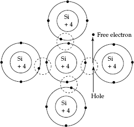
At the ambient temperature, some electrons may acquire sufficient energy equal to or greater than the forbidden band-gap energy EGand they will move to energy levels in the upper band. These electrons will be in an incompletely filled band and they can contribute to electrical conduction. While the electrons move to the Conduction Band, they leave Holes in the Valence Band (Holes were formed due to the formation of Hole–electron pairs during the process of breakage of covalent bands in Valence Band). Hole will have positive charge. Formation of Hole–electron pairs is shown in Fig. 2.6.

Fig. 2.6 Formation of hole–electron pair Conductivity of ‘intrinsic semiconductor’ is due to the Hole–electron pairs formed during broken covalent bonds or due to supply of energy to free electrons to cross the forbidden band gap to enter the Conduction Band.
Resistivity of semiconductor material can be expressed as
![]()
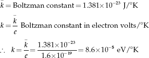
where A is a coefficient that varies slightly with temperature, and ρ is the resistivity of the emiconductor material. It is a function of temperature T and forbidden band-gap energy ΔEG.

Resistance across a standard mass and shape of a material at a given temperature is called the resistivity of the material. The reciprocal of resistivity is conductivity (σ).