Classification Of Materials
When voltages are applied, materials offer different values of electrical resistances to the passage of currents through them. On the basis of electrical resistances, materials are classified as conductors, semiconductors and insulators.
In solids, available energy states for the electrons form ‘bands of energy levels’ instead of discrete energy levels in atoms.
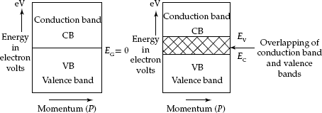
Conductors: Materials with adjacent or over-lapped conduction and Valence Bands with zero forbidden band-gap energy (EG = 0) are known as conductors. EBD for a conductor material is shown in Fig. 2.7.

Fig. 2.7 Energy-band diagrams for conductors
Initially, the energy levels in the Conduction Band are empty. But, electrons enter the Conduction Band due to increase in temperature or energy acquired from an applied electric field. Then the electrons move freely inside the Conduction Band as charge carriers with each electron carrying an electron charge qn = 1.6 × 10⁻¹⁹ C. So in a conductor, electric current can flow freely. Most familiar conductors are metals such as gold, silver and copper.
Semiconductors: Materials with small forbidden band-gap energy (EG), around 1 eV, re called semiconductors. Silicon, Germanium and gallium arsenide are semiconductor materials. They are also known as intrinsic or pure semiconductor materials.
Semiconductor materials have some of the following features:
- Typical value of resistivity is of the order 0.6 Ω-m at the room temperature.
- The material has negative temperature coefficient of resistance. Resistance of the semiconductor material decreases with increasing values of temperatures.
- The addition or doping of trivalent or pentavalent materials to the intrinsic semiconductors (Silicon or Germanium) modulates the electrical conductivity σ of the semiconductor materials. This is the important feature for the fabrication of P- and N-type semiconductors, which are the backbone materials for semiconductor devices in electronic engineering technology.
- At 0°K, EG0 = 1.12 eV for a Silicon semiconductor material.
- For Germanium semiconductor, EG0 = 0.785 eV.
- EG0 = 1.41 eV for gallium arsenide.
- At room temperature (300°K), EG = 1.1 eV for Silicon semiconductor.
- EG = 0.72 eV for Germanium semiconductor.
- Forbidden band-gap energy
![]()
- At very low temperatures, the Conduction Band is practically empty. When the temperature is increased, the electrons in the top of Valence Band acquire sufficient thermal energy and move into the Conduction Band.
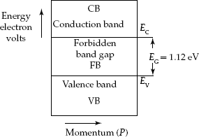
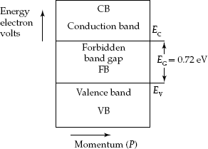
EG is forbidden band-gap energy, EC is the energy of the lower most energy level of Conduction Band and EV is the energy of the top most energy level of Valence Band.
Silicon semiconductor has the forbidden bandgap energy EG = 1.12 eV (Fig. 2.8). EBD for the Germanium semiconductor material is shown in Fig. 2.9. It has band-gap energy EG = 0.72 eV.

Fig. 2.8 Energy-band diagram for silicon semiconductor

Fig. 2.9 Energy-band diagram for germanium semiconductor
- Silicon has wider forbidden band-gap energy compared with Germanium semiconductor material. This suggests that Silicon devices work up to higher temperatures with stable operation. Silicon devices are preferable for military and tropical country applications.
- Because of smaller forbidden band-gap energy, Germanium devices are limited to lower temperature applications.
- Typical band-gap energy in semiconductors is less than 2 eV.
Insulators: The materials with large forbidden band-gap energy EG > 6 eV do not support conduction at all. Large forbidden band-gap energy between the Valence Band and the Conduction Band shown in Fig. 2.10 suggests that no electron can reach the Conduction Band. Such materials are known as insulators.

Fig. 2.10 Energy-band diagram for insulator materials
Insulators practically have no free electrons to act as charge carriers to support electrical conduction. Non-metallic solids such as glass, porcelain and mica behave as insulators. Their resistivity is very high, while conductivity is very low.